
Author Affiliations
Abstract
1 State Key Laboratory of Integrated Optoelectronics, Institute of Semiconductors, Chinese Academy of Sciences, Beijing 100083, China
2 Center of Materials Science and Optoelectronics Engineering, University of Chinese Academy of Sciences, Beijing 100049, China
3 School of Electronic, Electrical and Communication Engineering, University of Chinese Academy of Sciences, Beijing 100049, China
4 College of Materials Science and Optoelectronic Technology, University of Chinese Academy of Sciences, Beijing 100049, China
A quadrature phase-shift keying (QPSK) coherent photodetector chip consisting of a multimode interference 90° optical hybrid and a four-channel evanescent photodetector array is designed and fabricated with its photo-response in the L-band characterized. The metal organic chemical vapor deposition regrowth method is adopted to realize active–passive monolithic integration. The chip exhibits a low dark current below 100 nA for each photodetector in the array, a low excess loss of 0.85 dB, a common mode ratio rejection better than 13.6 dB, and a phase deviation within over the 40 nm wavelength span.
hybrid photodetectors monolithic integration photo-response Chinese Optics Letters
2023, 21(1): 011301
Author Affiliations
Abstract
1 School of New Energy, North China Electric Power University, Beijing 102206, China
2 State Key Laboratory of Information Photonics and Optical Communications, University of Posts and Telecommunications, Beijing 100876, China
With the incorporation of noble metal materials, photonic crystal fibers (PCFs) could be performed as an effective platform for refractive index sensing of the filling analytes. Furthermore, by coating functional dielectric layers upon the metal surfaces, the resonance energy transfer is modulated from the core mode of the PCFs towards the surface plasmon resonance mode of the metals, and the sensing performance could be boosted. Here, considering that the exciton-plasmon coupling is efficient between perovskite quantum dots (QDs) and gold, a kind of CsPbBr3 QDs/Au bilayer coated triangular-lattice PCFs has been simulated numerically as the refractive index sensors. With the optimization of the QDs and gold layer thicknesses, together with the variation of the central hole size of the PCFs, in the refractive index (RI) region of 1.26 to 1.34, a rather narrow full width at half maximum (FWHM) of the loss spectra was achieved as 13.74 nm when the central hole size was 1.28 μm and the highest figure of merit was 63.79 RIU (the central hole size was 1.53 μm). This work demonstrates that the analyte identification accuracy was enhanced by FWHM narrowing of the loss spectra; in addition, taking the abundance of the material choice of perovskite QDs into consideration, more analytes could be detected effectively. Moreover, by adopting asymmetric structures, the sensitivity of the PCFs based refractive index sensors could be further improved.
Photonic crystal fibers perovskite quantum dots refractive index sensor narrow FWHM Photonic Sensors
2022, 12(3): 220309
1 中国科学院半导体研究所 集成光电子学国家重点实验室,北京 100083
2 中国科学院大学 材料科学与光电技术学院,北京 100049
3 中国科学院大学 电子电器与通信工程学院,北京 100049
在越来越多的光子计数应用中,用于近红外光波长领域的单光子探测器受到广泛关注。例如在量子信息处理、量子通信、3D激光测距(LiDAR)、时间分辨光谱等光子计数应用领域。文中设计并展示了用于探测1 550 nm波长光子的InGaAs/InP单光子雪崩二极管(SPAD)。这种SPAD 采用分离吸收、过渡、电荷和倍增区域结构 (SAGCM),在盖革模下工作时具有单光子灵敏度。SPAD的特性包括随温度范围223~293 K变化的击穿电压、暗计数率、单光子检测效率和后脉冲概率。25 μm 直径的 SPAD 显示出一定的温度相关性,击穿电压随温度的变化率约为100 mV/K。当SPAD在盖革模式下温度为223 K工作时,在暗计数率为4.1 kHz,后脉冲概率为3.29%的基础上,对1 550 nm光子实现了21%的单光子探测效率。文中还分析和讨论了SPAD温度相关性的单光子探测效率、暗计数率和后脉冲概率的来源和物理机制。这些机制分析、讨论和计算可以为SPAD的设计和制备提供更多的理论支持和依据。
单光子探测器 温度相关性 光子探测效率 暗计数率 后脉冲概率 single-photon detector temperature dependency photon detection efficiency dark count rate after pulse probability 红外与激光工程
2021, 50(11): 20210453
1 南昌大学机电工程学院, 江西 南昌 330031
2 中国科学院苏州生物医学工程技术研究所江苏省医用光学重点实验室, 江苏 苏州 215163
3 江苏省医疗器械检验所, 南京 210019
为了对具有陡峭轮廓的物体进行非接触式表面粗糙度测量,常采用共聚焦成像对物体进行分层成像,进而重建出物体的表面三维轮廓,并采用高斯滤波的方法从表面三维轮廓中滤出粗糙度轮廓。在滤波过程中,会出现边界数据的缺失,常规的简单延伸原始轮廓两端数值的方法会导致滤波后的轮廓两端出现失真,该方法只适用于整体轮廓较为平缓的零件。引入了一种新的边界区域修正方法,该方法对表面弧度变化较大的零件也同样适用,能够准确提取物体的粗糙度轮廓。对整体轮廓较为平缓和陡峭的两组粗糙度样本分别进行共聚焦成像测量,对于整体轮廓较为平缓的样本,利用常规方法处理后,得到的均方根误差和粗糙度的平均值分别为0.080和2.86 μm,与该样本粗糙度值2.94 μm相比,相对误差为2.72%;利用边界区域修正方法处理后,得到的均方根误差和粗糙度的平均值分别为0.090和2.85 μm,与该样本粗糙度值的相对误差为3.06%。整体轮廓较为陡峭的样本的粗糙度值为3.2 μm,利用常规方法处理后,得到的均方根误差和粗糙度的平均值分别为0.120和3.31 μm,与该样本粗糙度值的相对误差为3.48%;利用边界区域修正方法处理后,均方根误差和粗糙度的平均值分别为0.045和3.19 μm,与该样本粗糙度值的相对误差为0.31%。研究结果表明,该方法能准确地测量整体轮廓较为陡峭的物体的表面粗糙度,为激光共聚焦粗糙度测量设备的研制提供了参考。
测量 非接触式测量 表面粗糙度 共聚焦成像 轮廓滤波器 激光与光电子学进展
2020, 57(21): 211203
1 中国人民公安大学,北京 100038
2 北京卓立汉光有限公司,北京 101102
为实现现场残留手帕纸塑料包装袋的检验区分,利用拉曼光谱法对35个不同品牌、不同系列、不同颜色的样本进行检验,依据拉曼光谱的差异,基于欧氏距离结合K均值聚类法,可将手帕纸塑料包装袋样本加以区分,同时考察了该法的重现性及分类可靠性。该检测分类方法不破坏检材,重现性好,分类客观性强,容错率高。为后续快速检验区分现场提取到的污染易损残片提供了理论依据。
拉曼光谱法 K均值聚类法 手帕纸塑料包装袋 Raman spectroscopy K-means clustering Plastic Handkerchief Paper Packaging Bag

Author Affiliations
Abstract
1 State Key Laboratory of Information Photonics and Optical Communications, Beijing University of Posts and Telecommunications, Beijing 100876, China
2 Guangxi Key Laboratory of Wireless Wideband Communication and Signal Processing, Guilin 541004, China
3 College of Optical Sciences, The University of Arizona, Tucson, Arizona 85721, USA
4 e-mail: dabombyh@aliyun.com
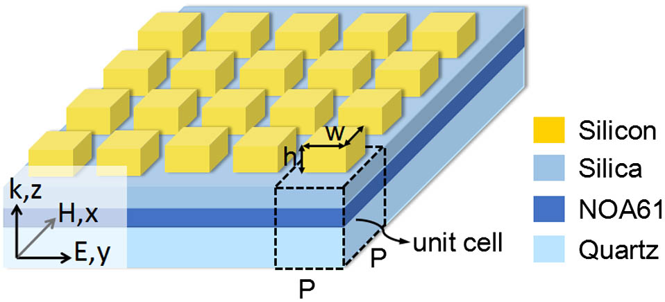
Metasurfaces have pioneered a new avenue for advanced wave-front engineering. Among the various types of metasurfaces, Huygens’ metasurfaces are thought to be a novel paradigm for flat optical devices. Enabled by spectrally overlapped electric resonance and magnetic resonance, Huygens’ metasurfaces are imparted with high transmission and full phase coverage of , which makes them capable of realizing high-efficiency wave-front control. However, a defect of Huygens’ metasurfaces is that their phase profiles and transmissive responses are often sensitive to the interaction of neighboring Huygens’ elements. Consequently, the original assigned phase distribution can be distorted. In this work, we present our design strategy of transmissive Huygens’ metasurfaces performing anomalous refraction. We illustrate the investigation of Huygens’ elements, realizing the overlapping between an electric dipole and magnetic dipole resonance based on cross-shaped structures. We find that the traditional discrete equidistant-phase design method is not enough to realize a transmissive Huygens’ surface due to the interaction between neighboring Huygens’ elements. Therefore, we introduce an extra optimization process on the element spacing to palliate the phase distortion resulting from the element interaction. Based on this method, we successfully design unequally spaced three-element transmissive metasurfaces exhibiting anomalous refraction effect. The anomalous refractive angle of the designed Huygens’ metasurface is 30°, which exceeds the angles of most present transmissive Huygens’ metasurfaces. A transmissive efficiency of 83.5% is numerically derived at the operating wavelength. The far-field electric distribution shows that about 93% of transmissive light is directed along the 30° refractive direction. The deflection angle can be tuned by adjusting the number of Huygens’ elements in one metasurface unit cell. The design strategies used in this paper can be inspiring for other functional Huygens’ metasurface schemes.
Photonics Research
2019, 7(12): 12001501
1 中国科学院半导体研究所 集成光电子学国家重点实验室, 北京 100083
2 中国科学院大学 电子电气与通信工程学院, 北京 100049
3 中国电子科技集团公司第四十四研究所 化合物半导体光电子事业部, 重庆 400060
通过测量平面型InGaAs/InP雪崩光电二极管闭管扩散器件帽层InP中Zn杂质的分布, 拟合出掺杂浓度随扩散深度的变化函数, 并且利用离化积分研究不同倍增层厚度下的最佳刻蚀坑深度和最佳刻蚀方法.结果表明在帽层深度不变的情况下, 最佳刻蚀坑深度会随着倍增层厚度而变化, 当倍增层厚度为1 μm左右时刻蚀坑深度在0.1~0.3 μm之间.采取反应离子刻蚀可以获得良好的刻蚀坑形貌, 有利于边缘击穿的抑制.
雪崩光电二极管 光探测器 离化积分 电场击穿 刻蚀 反应离子刻蚀 盖革计数 Avalanche photodiodes Photodetectors Ionization integral Electric breakdown Etching Reactive ion etching Geiger counters
Author Affiliations
Abstract
1 State Key Laboratory of Information Photonics and Optical Communications, Beijing University of Posts and Telecommunications, Beijing 100876, China
2 School of Science, Beijing University of Posts and Telecommunications, Beijing 100876, China
We propose and numerically investigate an efficient transmission-mode metasurface that consists of quasi-continuous trapezoid-shaped crystalline silicon nanoantennas on a quartz substrate. This metasurface provides a linear phase gradient and realizes both full 2π phase shift and high transmission efficiency in the operating wavelength range from 740 to 780 nm. At the central wavelength around 751 nm, the total transmission efficiency is up to 88.0% and the section of the desired anomalous refraction is 80.4%. The anomalous refraction angle is 29.62°, and larger refraction angle can be achieved by changing the period of the super cell. We demonstrate a refraction angle as large as 38.59°, and the anomalous transmission efficiency reaches 76.6% at wavelength of 741 nm. It is worth mentioning that the structure is much simpler than conventional metasurfaces based on arrays of discrete nanoantennas. Our research may pave the way for designing efficient all-dielectric phase-gradient metasurfaces and applying them in integrated optical devices for wavefront control.
Metamaterials Phase shift Integrated optics devices Photonics Research
2018, 6(6): 06000517
1 中国科学院半导体研究所 集成光电子学国家重点实验室, 北京 100083
2 中国科学院大学 电子电气与通信工程学院, 北京 100049
InGaAs/InP盖革模式雪崩光电二极管(APD)阵列的性能与阵列片内均匀性密切相关。阵列面元的主要结构参数有倍增区厚度、电荷层厚度和掺杂浓度、吸收区的厚度以及器件工作的过偏压。它们的不一致性不仅会造成器件本身性能的差异, 还为后续的读出电路带来了巨大的挑战。通过研究APD结构参数变化对其击穿电压(Vbreak)、暗计数率(DCR)和单光子探测效率(PDE)的影响, 将APD阵列面元间击穿电压波动控制在±1V以内, 使暗计数率和光探测效率的波动小于10%, 从而得到不同温度下各个结构参数的最大允许波动值,确定了每个温度下制约器件性能的主要因素,为大规模、高性能盖革模式雪崩光电二极管阵列的材料生长和工艺制备提供了理论依据。
盖革模式 雪崩光电二极管 阵列 均匀性 Geiger mode InGaAs/InP InGaAs/InP avalanche photodiode array uniform

Author Affiliations
Abstract
State Key Laboratory of Information Photonics and Optical Communications, Beijing University of Posts and Telecommunications, Beijing 100876, China
A novel scheme for the design of an ultra-compact and high-performance optical switch is proposed and investigated numerically. Based on a standard silicon (Si) photonic stripe waveguide, a section of hyperbolic metamaterials (HMM) consisting of 20-pair alternating vanadium dioxide (VO2)/Si thin layers is inserted to realize the switching of fundamental TE mode propagation. Finite-element-method simulation results show that, with the help of an HMM with a size of 400 nm×220 nm×200 nm (width×height×length), the ON/OFF switching for fundamental TE mode propagation in an Si waveguide can be characterized by modulation depth (MD) of 5.6 dB and insertion loss (IL) of 1.25 dB. It also allows for a relatively wide operating bandwidth of 215 nm maintaining MD>5 dB and IL<1.25 dB. Furthermore, we discuss that the tungsten-doped VO2 layers could be useful for reducing metal-insulator-transition temperature and thus improving switching performance. In general, our findings may provide some useful ideas for optical switch design and application in an on-chip all-optical communication system with a demanding integration level.
Optical switching devices Integrated optics devices Metamaterials Photonics Research
2017, 5(4): 04000335


